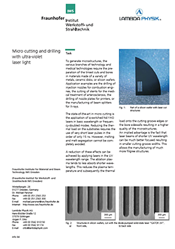

Report describing the use of a Q-switched UV laser for the micro-cutting of silicon. Laser parameters are provided and examples are given of laser-cut 16 m wide grooves in a wafer of 220 m thickness. The technique allows for the creation of the tiniest cuts and bores in materials made of a variety of Materials e.g. metals ceramic disks or silicon wafers. To generate microstructures the various branches of technology and medical technologies require the preparation of the tiniest cuts and bores in materials made of a variety of metals ceramic disks or silicon wafers. Application examples are the drilling of injection nozzles for combustion engines the cutting of stents for the medical treatment of arteriosclerosis the drilling of nozzle plates for printers or the manufacturing of beam splitters for X-rays. The state-of-the-art in micro cutting is the application of q-switched Nd:YAG lasers in basic wavelength or frequency- doubled modes. Reducing the thermal load on the substrates requires the use of very short laser pulses in the order of only 15 ns. However melting and melt segregation cannot be completely avoided. A reduction of these effects can be achieved by applying lasers in the UV wavelength range. The ablation plasma tends to less absorb shorter wavelengths. This reduces the plasma temperature and subsequently the thermal load onto the cutting groove edges or the bore sidewalls resulting in a higher quality of the microstructures. An implied advantage is the fact that laser beams of shorter UV wavelength can be much better focused resulting in smaller cutting groove widths. This allows the manufacturing of much more filigree structures. The Lambda Physics AG and the Fraunhofer IWS jointly developed the prototype of a UV wavelength microstructuring machine for cutting and drilling of various parts and components. The heart of the machine is a q-switched and diode-pumped solidstate laser with frequency tripling. The unit is a stable and low-maintenance industrial laser of the type GATOR UV with the following beam parameters:- Wavelength 355 nm - Repetition frequency 10 kHz - Pulse length 15 ns - Average power 3 W - Beam quality close to TEM00. The machine is equipped with a UV scanner and plane field optics with a working area of 100 · 100 mm2. The laser beam is switched by galvanic shutters instead of turning the laser power on and off. Subsequently the laser is working continuously in thermal equilibrium conditions ensuring highest beam quality. The small compact design of diode-pumped solidstate lasers allows the design of a tabletop unit. With the above-described unit lasercutting tasks on silicon wafers have been performed. The high beam quality makes it possible to generate cutting groove widths of 16 m at a wafer thickness of 220 m. The cutting process can be described as sublimation cutting because cutting of silicon does not generate much melt. Accretions of silicon oxide can be easily removed in an ultrasonic bath.
View Document (140Kb)
Copyright of ©2006 Fraunhofer Institute IWS Dresden
We make every effort to trace copyright. If inadvertently we have not attributed copyright or attributed it incorrectly, please contact us using our webform or by emailing dlm@ailu.org.uk and we will rectify the situation.
Disclaimer
To view disclaimer details click here